[TOC]
# Chapter 1 - WebFPGA Quick Start Guides ## 1.1 WebFPGA Quick Start Guide - FPGA Shasta Board
After days of anxious anticipation, a neatly packaged white parcel arrives at your doorstep. Oh what's that? "WebFPGA", it reads.
Today, you have received your WebFPGA kit. Oh boy.
After connecting the slim, red PCB to your computer's USB port, you witness an orange, blinking LED. Seems like once a second.
Pressing the white on-board button seems to change the rate of blinking. That's interesting, you note. But it's time to move on to bigger and better things.
You're ready to begin building your own applications.
Hopefully that wasn't too melodramatic. But we're excited. And we hope that you're excited too! Let's run some examples before you get ahead of yourself.
If you are running on Linux, you need to install a udev rule in order
for the user space to have read/write permissions to the board (linux-udev-rules).
Make sure to reload the rules with sudo udevadm control --reload-rules && sudo udevadm trigger.
Even if you plan on using offline tools, the Web IDE is a convenient home to example code. You can use it to ensure that your hardware is functioning properly. Open the Web IDE using Google Chrome or Opera: beta.webfpga.io
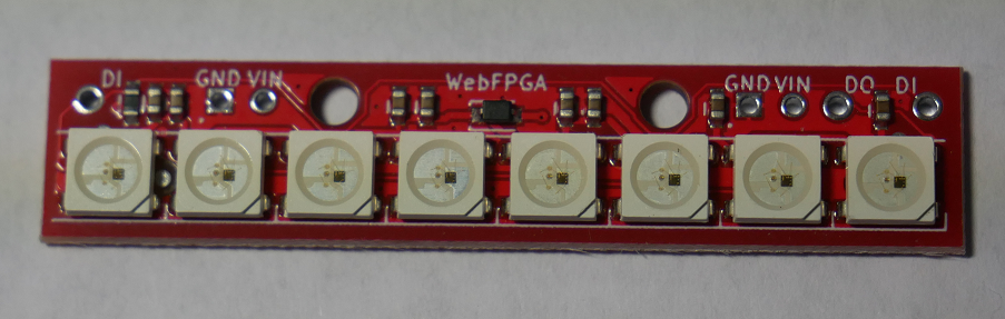
Easily, the most eye-catching example is the on-board Neopixel RGB LED.
Load the example named WF_neopixelx1_fading_demo.v and click Run Synthesis.
Wait for up to two minutes for synthesis to complete. After the console
outputs Bitstream ready, click Flash Device.
(Note: The x1 in the filename indicates that the code controls a single
Neopixel LED. x8 refers to the Neopixel peripheral strip.)
Now the board should pulsing with a pleasing RGB pattern.
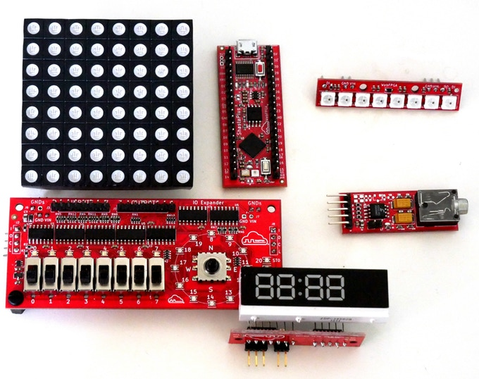
After you have the on-board examples running, it's time to move on to the kit peripherals.
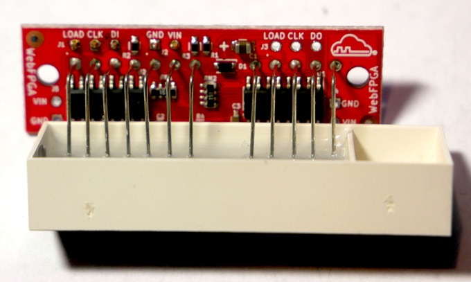
We will outline connecting the modules together using a breadboard. There are other methods, but breadboards are visually simple and require no jumper wires.
Each peripheral in your kit will need male headers soldered on to allow for insertion into the breadboard. But be careful! You don't need to solder pins to every single pin — in fact, that will actually make insertion more difficult.
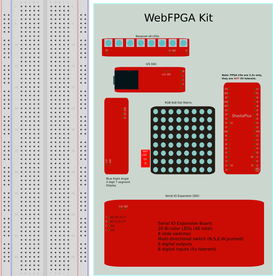
Use the above image as a reference to which pins you should solder.
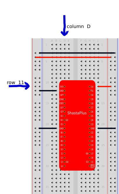
After you've soldered those modules, insert the main device into the breadboard,
aligning the top-left pin into Row 11 and Column D.
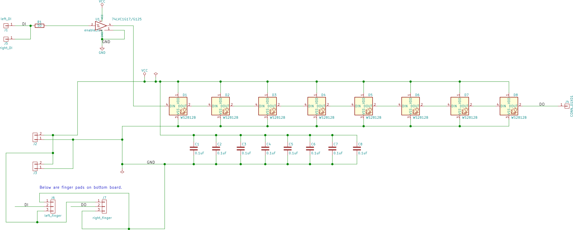
Then, once the main board is secured on the breadboard, it's time to connect a couple of modules. In this post, we will be connecting the Neopixel Strip, the 7-Segment Display, and the Audio DAC.
Everything has been designed to fall neatly into place. The power and ground pins will align with the rails on the breadboard. The data pins will align with the appropriate FPGA board pins.
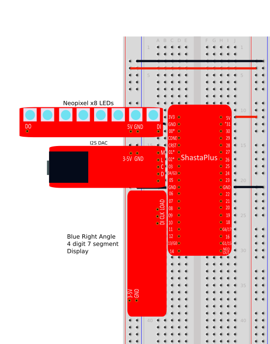
After these three peripherals are secured, you can run several examples:
neopixelx8_random_demo.v — Cycles random colors on the Neopixel Strip.WF_7seg_clock_time.v— Increments the display once a second. Pressing
the white push button (or Web Button 1) will start/stop the counting.WF_7seg_timer_demo.v— Operates the display as a stopwatch. Pressing
the white push button (or Web Button 1) will clear/start the display.Verilog was first implemented as a verification and modeling tool for digital logic designs. The modeling and design portion is called HDL (hardware descriptive language). Prior to HDL the digital logic design was done with schematics of logic elements from your fabrication house who in the end manufactured your silicon ICs (integrated circuit). Most of these devices where either gate array or custom ICs, referred to as ASICs (application specific IC). As a separate development path, FPGAs (field programmable gate array), CPLDs (complex programmable logic device) and PALs (programmable array logic) had their own design languages and tools, most being proprietary to the manufacture and their product lines.
As verilog became the norm for verification in the ASIC design world. Designers started using a subset of the verilog language to just describe and model the digital logic. These models are independent of the verification aspect of digital design for which verilog was developed.
Along came tools to synthesis the digital design models into a gates and flip flops mapped to a manufacture's library and processes. This only worked if a restricted subset of verilog was used in the model, or now the actual design of the logic.
This restrictive subset of verilog is referred to as RTL (register transfer level). Our introduction that follows will only cover the RTL portion of verilog. Guides and recommendations will be based on best practices and keeping the designs simple and straight forward.
We caution the reader to know that googling verilog will find verification and model examples as well as RTL examples. Only the RTL portion of verilog can be included in synthesizable verilog for use in FPGAs and ASICs.
## 2.2 Your First Verilog ModuleIn this section we will introduce you to your first verilog based design using the WebFPGA web site. The basic design unit in verilog is the module structure. All designs have a least one module, most will have multiple modules.
moduleA verilog module defines the digital circuits within your design. Below is example of a module, it has inputs, outputs and the digital design logic.

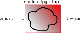
For our first WebFPGA verilog module we will connect the ShastaPlus FPGA board's push button switch to the user yellow LED. This is likely the simplest verilog module there is. It is assumed you have already tried out your WebFPGA ShastaPlus board with the website, if not see the quick start guide.
Here is a diagram of the module we will create.
Using the verilog code window on WebFPGA site, enter the following.
module fpga_top(input WF_BUTTON, output WF_LED);

    assign WF_LED = WF_BUTTON;

endmodule
After typing in the module go ahead and run synthesis and flash the bitstream onto the ShastaPlus. If everything went well, then pushing the white button on ShastaPlus will turn on the yellow LED.
If you are having any syntax error issues, pay attention to the semi-colons in the above verilog code.
module syntaxModules are defined with the keyword module, and ended with the keyword endmodule.
Note that there isn't a ; after the endmodule.
The name of the module follows the module keyword. WebFPGA 1.0 uses fpga_top for all the top level module names. This helps tell the IDE which module is the top most module. Although not a verilog requirement its a best practice to use the word top in the top most module. In the next few examples we will be using only one module, we will cover multiple modules later. Only signals that are on the top most module can become external FPGA signals.
After the name is the IO list for the module. These IOs are called signals. Here you list each signal and the direction associated with the signal. The direction reference point is the module, so WF_LED signal is an output of the module. Also, since this in the top most module, WF_LED is also an output from the FPGA device on the ShastaPlus board.
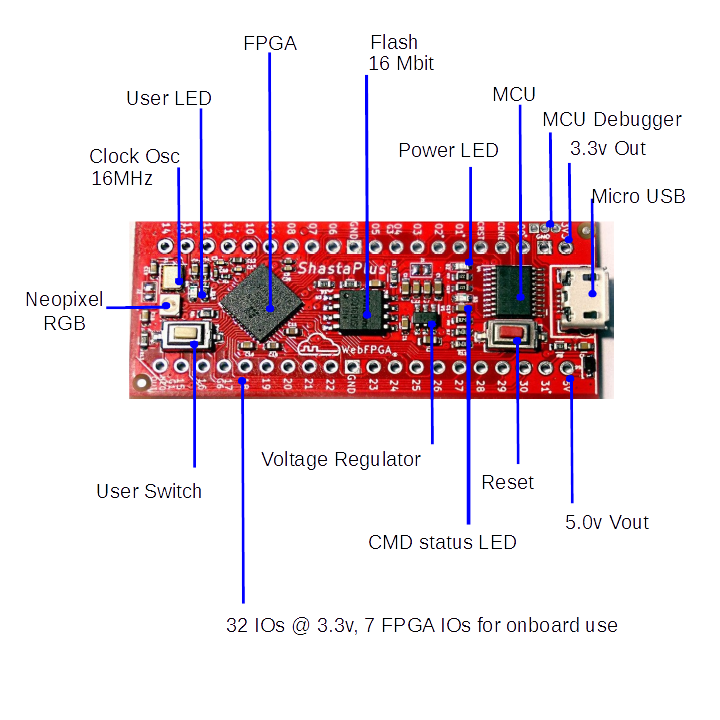
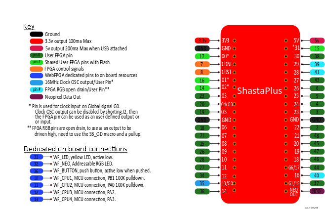
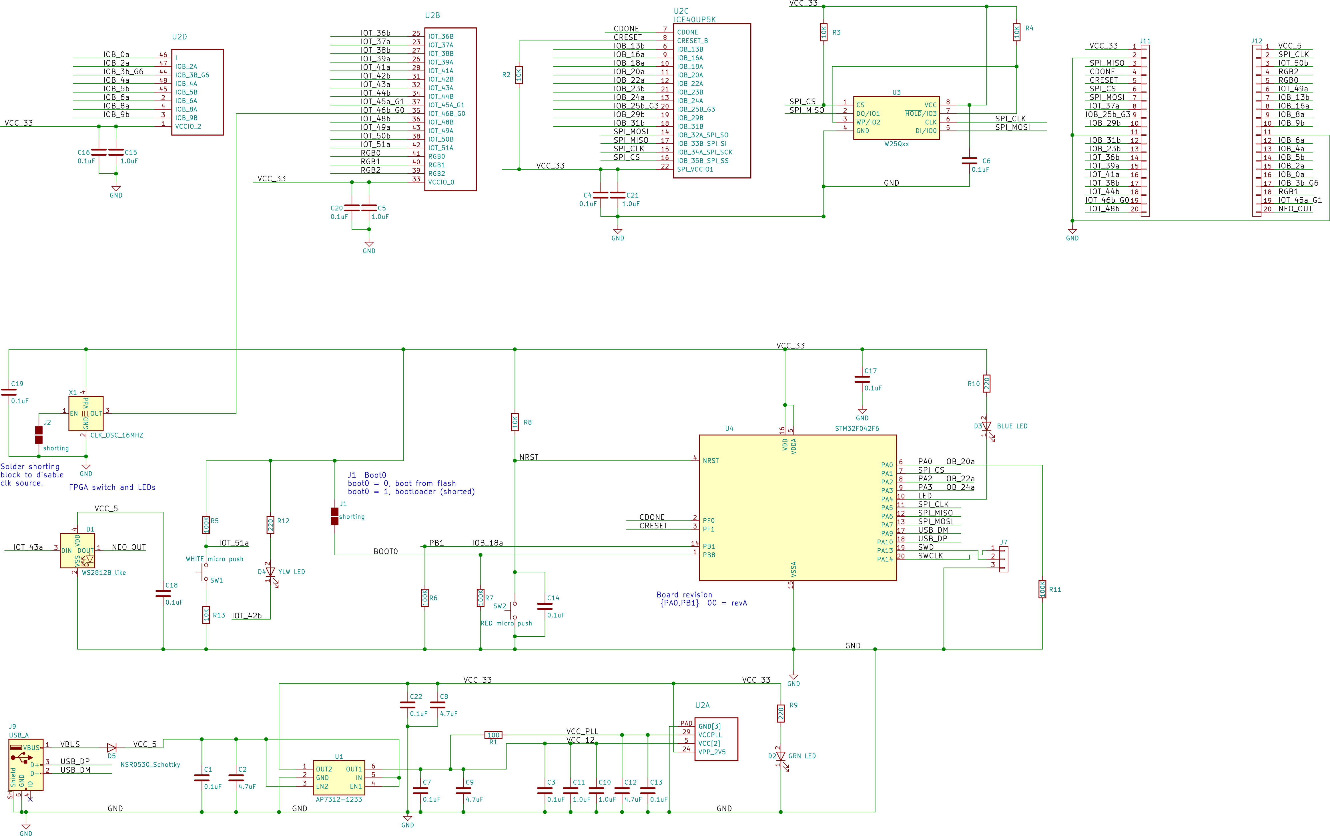
As a best practice, WebFPGA examples will always capitalize the signals which will be IOs on the FPGA device. This helps the reviewer understand which signals will become external IOs. Also every dedicated external IO on ShastaPlus will have the prefix WF_. See ShastaPlus board pinout in Appendix A, for the dedicated signals.
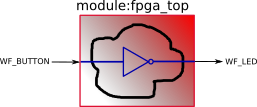
assign keywordIn our block diagram for a module, the center had a cloud of "digital logic stuff". In our module our "stuff" is just the assign statement. The keyword assign is used to assign a signal to some digital logic. This logic must be combinational only.
So what is combinational logic?
Combinational logic is a Boolean circuit where the results are dependent only on the current inputs. This boils down to not using time dependent circuits such as latches and flip flops which have a clock associated with them. So we can use the Boolean operators like and, or, xor, and not to create our logic. Clock associated logic is referred to as sequential logic, or time-dependent logic. Combinatorial is sometimes used to mean the same as combinational. See the wiki for more details Combinational logic wiki.
assign WF_LED = WF_BUTTON;
Our assign statement takes the present state of the WF_BUTTON and connects that signal, without modification, to the WF_LED output signal. This becomes just a wire! Not a really good use of an FPGA device.
Let us add some logic to the equation. Change the assignment as shown below.
assign WF_LED = ~WF_BUTTON;
The results will show the LED is lit until the button is pushed. We added the not logic operator, ~.
What we have done is invert the WF_BUTTON signal and connected that result to WF_LED signal.
In summary we have created one of the most simple verilog module there is. Not very fancy but did cover the module/endmodule and assign keywords. The next section will go over other forms of the module keyword. Verilog has evolved over nearly 35 years. Unfortunately examples found on the internet don't automatically update to the most recent methods. This can cause confusion for the beginner looking to learn verilog, so the next section should help clarify these other methods.
In this section we will expand on our previous work with the module keyword.
Verilog was evolved over 35 years, and the module keyword had a major update in the verilog-2001 standard and is backwards compatible. So as a new user of verilog it is likely you will search internet for examples and you will come across the older methods. You can use both styles in the same design, thus making older libraries still useable.
Our prior example, in verilog-2001 style.
module fpga_top(input WF_BUTTON, output WF_LED);

    assign WF_LED = ~WF_BUTTON;

endmodule
Before verilog-2001, the designer had to specify the signals in multiple places as show below.
module fpga_top( WF_BUTTON, WF_LED);

  // signal direction
    input  WF_BUTTON;
    output WF_LED;

  // signal type
    wire WF_BUTTON;
    wire WF_LED;

    assign WF_LED = ~WF_BUTTON;

endmodule
If you want check the code, cut and paste it into the webFPGA verilog window and Run Synthesis. The above produces the very same bitstream. If you come across the older style, the code is perfectly fine to use.
Since we looked at the older more verbose style let us look at the signal type section. On lines 8 and 9, we declared the signals as wire. In the verilog-2001 style we didn't declare the signals with a type. By default, all signals are wire unless declared reg or a vector. For now don't dwell on the keyword reg, or vectors; we will cover that in a later example.
Earlier we said the assign statement required an assignment of combinational logic only. Signals that are declared as wires can only have combinational logic assignments. So if you plan to use the assign statement, the signal will need to be a wire either by declaring it, or letting verilog default it to wire.
A wire doesn't mean just a connection with no logic as in a jumper wire. Wires can have a Boolean equation associated with them. The inputs to the equation can come from various sources such as as other wires,the outputs of flip flops, external input signals, and others.
It is still correct to declare the type as wire as shown below.
module fpga_top(input wire WF_BUTTON, output wire WF_LED);

    assign WF_LED = ~WF_BUTTON;

endmodule
In the above module see the additional keyword wire included in the IO list.
As you can see the verilog-2001 syntax is cleaner and much easier to add additional signals. In the past adding an additional signal required updating the design code in three places. In large designs modules can have hundreds of signals.
When modules have many IOs it is a best practice to list the signals one signal per line. This helps finding signals amongst many files by using Linux shell commands such as grep, awk and sed. Our initial designs won't have a large amount of signals, but at some point you will encounter the style below.
module fpga_top(

  input  wire WF_BUTTON,
  output wire WF_LED
);

    assign WF_LED = ~WF_BUTTON;

endmodule
You can see that each signal is on one line, making shell commands that operate on one line very effective in searching for signals. We will cover using shell commands in a more advance tutorial.
Verilog is very flexible on the coding style. For example our module can be just one line.
module fpga_top(input wire WF_BUTTON,output wire WF_LED); assign WF_LED=~WF_BUTTON;endmodule
I am not recommending this style, it is just that the designer can create a style that will fit their needs. Go ahead and try it in webFPGA.
The module below is also valid verilog coding.
module
  fpga_top(
  input
    wire
    WF_BUTTON,
  output
    WF_LED
);
  assign
    WF_LED
    = ~WF_BUTTON;
endmodule
In this section we learned that a module declaration can look many different ways. They are all valid Verilog syntax. The designer or design team must choose what their preferred style to be used on a project if they want consistency. It is a best practice to choose a style to use and stay with it. Since verilog is very flexible and not strict, and therefore leveraging code from other sources the designer will encounter different styles.
We recommend this style and will try to make all our libraries conform.
module fpga_top(

  input  wire WF_BUTTON,
  output wire WF_LED
);

    assign WF_LED = ~WF_BUTTON;

endmodule
For our verilog examples, we may use the more compact coding to help focus on just the few lines that we want to explain. The next section will introduce the reg type and discuss the WF_blinky.v example from the webFPGA site.
reg Keyword and WF_blinky.v ExploredIn this section we will introduce the keyword reg by review of the WebFPGA example WF_blinky.v. Go to the website and load WF_blinky.v if its not already in the verilog window. Flash the ShastaPlus board and make sure the yellow LED is blinking at a rate of about one second on and one second off.

The above module diagram shows what we intend to design. A top down approach is used, define the requirements, then work on the input and output signals. This creates a blackbox in which the input and outputs are known but the contents are left for later. Even though this is a simple design it is a good practice to have a consistent method to designing even the simplest module, especially for newcomers to digital design.
Our requirement is for a signal to drive a LED, in a cyclical way, where it turns on the LED for one second, then turns it off for one second, then repeats.
Our only output signal we need is for the LED and will be WF_LED.
For the input this is less obvious for the first time designer. The above diagram uses WF_CLK for the input. WF_CLK is connected to a clock oscillator on the ShastaPlus FPGA board. For any serious digital design we need a clock for our logic.
So what is a clock?
You may already understand the term clock for electronics, however others may be new to the concept. When we hear clock, we may think of a wall clock, or a wrist watch, or a clock for microcontroller; they all keep a measure of time. Digital logic needs a clock to pace logic thru different states. Logic which uses a clock is called sequential logic versus combinational logic covered in the prior section.
Below is the waveform of the WF_CLK signal. The waveform diagram can also be called a timing diagram.
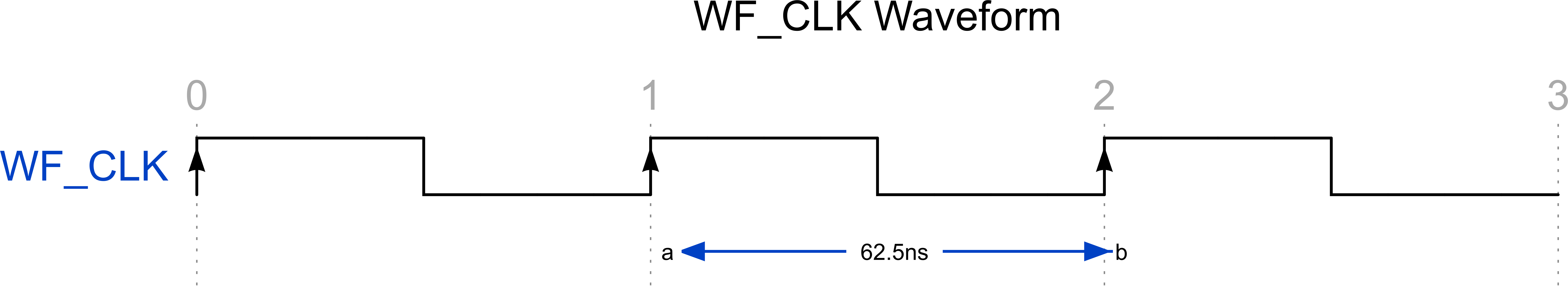
The WF_CLK waveform shows a 16MHz signal which is coming from a clock oscillator. The clock oscillator generates a signal which is switching from 0 volts to 3.3 volts, with a period of 62.5ns. A period is the length of the repetition cycle; i.e. from rising edge to rising edge as indicated by the arrows pointing up.
We will use these rising edges to pace our LED blinking circuit. WF_CLK becomes our time base for our design. Each time base or clock is also know as a clock domain, we will dive into clock domains later.
For those who do math,
16MHz, means 16 million cycles per second (rising edge to rising edge).
If $\bf f$ is our frequency, the period is $\bf \frac{1}{f}$, then $\bf \frac{1}{16x10^6} \Rightarrow $ 62.5ns is WF_CLK's period.
It is not necessary to create a timing diagrams for simple modules, however it is a good practice for more complex modules. Below is a timing diagram of our WF_blinky.v module showing the output signal WF_LED.
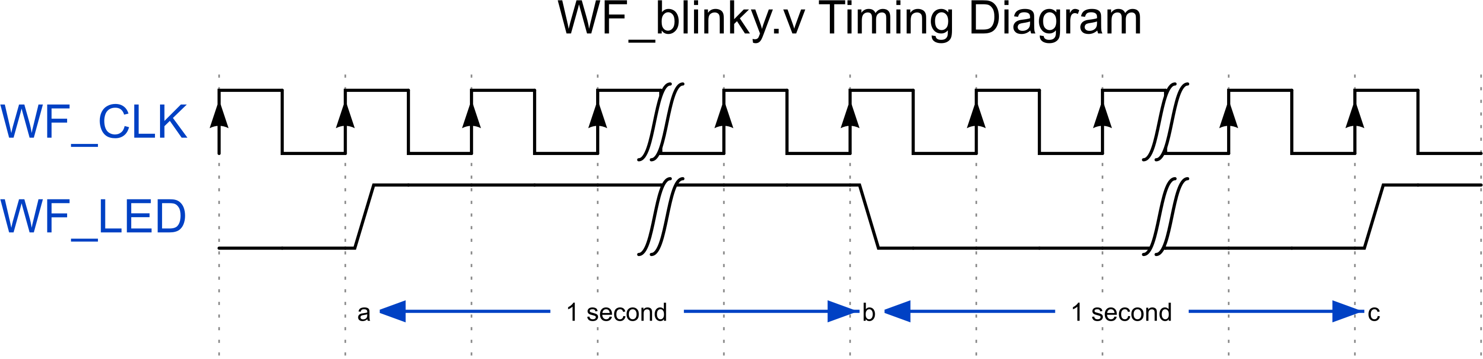
We are introducing timing diagrams here even for simple modules so that when we get to more complex modules the reader is familiar reviewing and understanding what they are showing. The above diagram has two squiggly lines indicating a long passage in time. Please note that the WF_LED signal changes only after a rising edges. We will point this out again when exploring WF_blinky.v's verilog code.
// WF_blinky.v
//
// The "Hello World" of Digital Logic!
// This example blinks the on-board user LED once a second.

module fpga_top(
    input  wire WF_CLK,
    output reg  WF_LED
);

    reg [23:0] counter;

    // Blink LED every 1000 ms
    always @ (posedge WF_CLK) begin
        // Try using a different value here...
        // 8000000 will cause it to blink twice as fast!
        if (counter == 16000000) begin
            WF_LED   <= ~WF_LED;
            counter  <= 'b0;
        end else begin
            counter  <= counter + 'b1;
        end
    end

endmodule
The verilog module above consists of three sections typical of every module.
The module header, which has the module name, fpga_top, and the IO list on lines 7 and 8. We covered this earlier.
Line 11 consists of the declaration of the internal module signals. This section is new.
Lines 14 thru 23 are the "digital logic stuff" of the module. The prior example only had a wire or single inverter. Below is just this section without comments.
 always @ (posedge WF_CLK) begin
     if (counter == 16000000) begin
         WF_LED   <= ~WF_LED;
         counter  <= 'b0;
      end else begin
         counter  <= counter + 'b1;
      end
  end
always keywordThe above code from the always keyword on line 1 to the end keyword on line 8 is a procedural block. The always procedural block differs from the assign statement in that the assign is continuous, while the always has a sensitivity list and only evaluates when the sensitivity is true.
There is a lot of stuff in the last sentence. We have already covered the assign keyword. With assign you create signals which are comprised of combinational logic with Boolean logic operators such and, or and not. In always procedural blocks, you create signals which are evaluated on a certain condition and then assign the value to a signal. I used the word assign to mean to transfer the evaluated value to the desired signal, do not confuse that with the assign keyword.
Breaking down the always statement.
always @ (sensitivity list) begin
end
The sensitivity list can be a combination of signals and conditions. For our initial examples we are going to use posedge with our clock, WF_CLK. The keywords begin and end are brackets to group multiple assignments for the particular condition. begin and end are optional if there is only one assignment in a group.
Earlier our WF_blinky.v timing diagram had a notation on it for a rising edge. We had defined our output signal to change only on a rising edge. The posedge in the sensitivity list is our condition for the rising edge. Therefore the procedural block will only evaluate on the rising edge (posedge) of our clock, WF_CLK.
In summary, on every rising edge of our clock, the bracketed verilog code will be evaluated and assigned.
 if (counter == 16000000) begin
     WF_LED   <= ~WF_LED;
     counter  <= 'b0;
  end else begin
     counter  <= counter + 'b1;
  end
Let us breakdown and review the above verilog code snippet. The begin and end are just bracketing groups of statement just like {} in C. If there is just one statement the brackets can be removed. Sometimes they are added for clarity, such as the begin/end pair on lines 4 and 6 as they are not needed.
The if/else statement is similar to other languages, the condition in the () must evaluate to Boolean TRUE or FALSE and can be any combinational equation.
reg keywordNow comes the counter and WF_LED signals. From a software standpoint we may like to say they are variables, from hardware point of view they are signals and registers. All three terms are used interchangeably, I can't say if one is better than the other, or which is more correct. It is not a debate for here. However for verilog they are type reg. The whole reason for this section was to introduce reg. We covered a lot, and have a lot more to cover.
Note: the statements below are very important, understand them.
If a signal, or variable is declared reg, this doesn't mean it is a register in a hardware point of view, such as a flip flop. All signals or variables assigned in the always procedural block must be declared a reg. You cannot use assign to assign a signal that was declared a reg.
Let us examine one line of the code within the always block.
counter <= counter + 'b1;
This line is similar to any other programming language, it is just adding one to the variable counter. However the equation has two likely new notations to most of you. The first is <= , and the second being 'b1.
The assignment operator <= is the non-blocking assignment. We recommend you always use non-blocking assignments within the always blocks. What this means, is every equation is evaluated in parallel and assigned according to the control logic. In this case the control logic is the rising edge of WF_CLK and the FLASE case of the if statement.
You can use = assignment operator, but it is not recommended. This is blocking and the behavior is like software in that statements are evaluated in order, this is best for modeling and verification of a digital logic block.
The constant 'b1 is just binary one. We want the value of the counter to increment by one. The + operator is an adder, so we are just adding one. The synthesizer will translate this into an incrementer at the hardware level since an incrementer uses less resources then a full adder. Right now we aren't worried about the amount of resources your code takes. It is always beneficial to understand how the code you are writing translates into actual hardware, however it is not necessary at this time of learning verilog. If you are planning a career in digital electronics understanding all the aspects of the final hardware is required.
Constants are an important part of verilog and they can be written in many ways. The following are all the same, they represent one, 1'd1, 1, 'b1, 1'b1, 1'h1, and 24'b1. We could use any of these in the line above. You should try it and see the results. The letter after the ' is the base, either decimal, hexadecimal, octal or binary. The number before the ' is the length in bits of the number. If the length, or size is left blank, then verilog will zero extend to match the size of the other operand. If verilog was strict, the constant would be 24'b1, 24'd1 or 24'h1 . The coder can use the more strict style, and should only use the zero extent feature when it applies. Zero extent feature is convenient in that if we changed the size of counter we would not need to update the size of the constant one.
Sizing the register counter is important, if sized too short the synthesizer will translate to something that the designer did not expect. If too long, well the synthesizer is pretty good in trimming excessive logic. For our module, we need to count 16 million rising edges to measure one second in time. It is a large number, and we need to declare it in bits. So we need to convert 16,000,000 decimal to binary to check its size in bits or use the bit size table in the appendix to size your reg declaration. We recommend you get a calculator for programmers to help converting to and from different bases. Converting to hexadecimal is a more compressed representation of binary and can infer how many bits our counter needs to be.
16,000,000 decimal $\bf \Rightarrow $ F4 2400 in hex $ \Rightarrow $ 24'hF4_2400.
From this we see we need a 24 bit counter, and we declared counter as a 24 bit register.
reg [23:0] counter;
We just introduced vectors in the above verilog snippet. Both reg and wire can be vectors, or a group of wires and registers. Within the [] two values are needed, one for the msb and the other for lsb of the vector. Vectors are evaluated as [msb:lsb] when doing compares. Also msb and lsb values can be positive, negative or zero, and there is no restriction of which is greater than the other.
This extra flexibility in defining your vectors makes all the following the same; defines a register of 24 bits. In the WF_blinky.v example you can change the declaration to match lines 2 or 3 and flash your ShastaPlus board. The blinking LED will still be at one second intervals.
reg [23:0] counter;
reg [0:23] counter;
reg [-5:19] counter;
When creating vectors use line 1 style, WebFPGA examples will only use line 1 style unless it is absolutely necessary to use something else. Just because you can do it, doesn't mean do it.
In a later section will show how to access bits within a vector, for now our example is using the entire vector as single unit.
We covered the else portion of the if statement, now let us review the TRUE case.
always @ (posedge WF_CLK) begin
    if(counter == 16000000) begin
        WF_LED   <= ~WF_LED;
        counter  <= 'b0;
    end else begin
        counter  <= counter + 'b1;
end
The if condition becomes TRUE when the counter is equal to 16 million. We already saw that the counter will increment by one if the counter wasn't equal to 16 million. Remember this verilog snippet is only evaluated on the rising edge of the WF_CLK signal. Each rising edge represents 62.5ns in time. Multiplying 62.5ns by 16M gives us one second. We didn't need to do this math because we know the clock source is 16MHz, therefore we know 16 million cycles is one second.
Once the compare is TRUE, i.e. one second has passed, the following two lines of verilog code are evaluated in parallel. We are using <=, the non-blocking assignment operator, so evaluations occur in parallel.
    WF_LED   <= ~WF_LED;
    counter  <= 'b0;
Don't fret over the evaluations in parallel, it is quite simple. Both WF_LED and counter values will be evaluated on the same rising edge of the WF_CLK. This behavior is one of the big differences between regular programming languages and verilog. The performance advantage is huge.
The following is a word description of what will occur.
On the rising edge of WF_CLK in which the counter is equal to 16 million (24'hF4_2400), WF_LED signal will become the opposite of what it currently is, and counter will become 0.
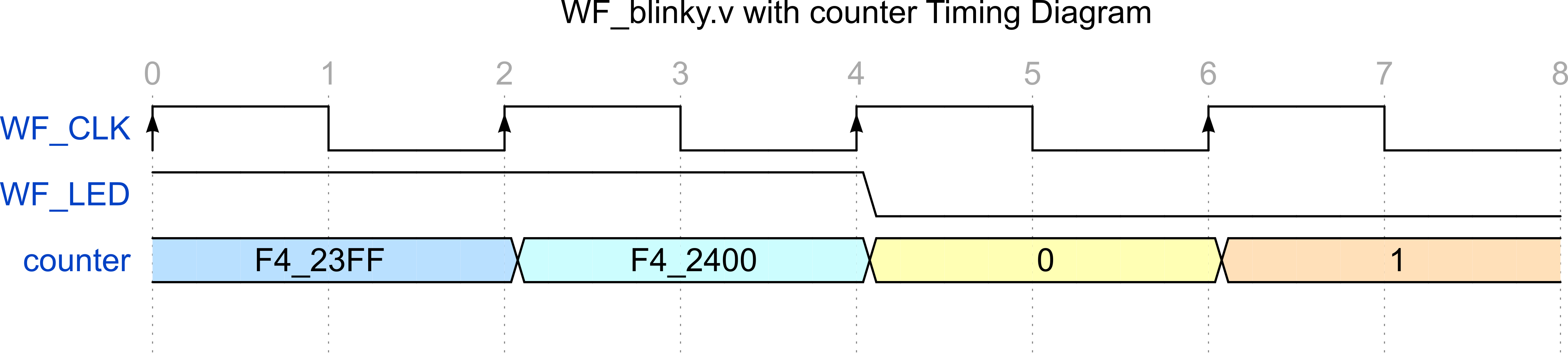 From the above timing diagram find the rising edge with the marker 4 above it. On this rising edge you can see that the signal
 WF_LED toggled, and the counter value changed to zero. All this occurred at the same time or in parallel, once the compare was TRUE.
Since WF_LED is being assigned within the always procedural block the signal must be declared a reg. This is done in the module's IO list, shown below. In the prior example when we connected the push button with the LED, WF_LED was declared as a wire because it was assigned with the assign keyword.
module fpga_top(
    input  wire WF_CLK,
    output reg  WF_LED
);
We stated earlier that just because we declare a signal as reg doesn't imply a storage element such as a flip flop. In our example we use the condition posedge in the sensitivity list, with this condition a flip flop will be inferred. Synthesis will map this storage element to a rising edge D style flip flop. Later we will review the behavior of a D style flip flop.
We covered a lot in this section. It is advisable to re-read this section again as many topics were covered all relating to reg. A good grasp of the topics is needed to be successful in using verilog to design digital circuits. With the always block we can design sequential logic blocks, the heart of all digital circuits. The assign statement allows us to connect and add Boolean logic between various design blocks. In the next section we will introduce how to use multiple always blocks to enhance the WF_blinky.v design. These enchantments will lay the ground work on how to architect your digital logic design into simple digital blocks.
| Acronym | Definition | Comment |
|---|---|---|
| ASIC | application specific IC | |
| CPLD | complex PLD | |
| FPGA | field-programmable gate array | |
| HDL | hardware description language | |
| IC | integrated circuit | |
| IO | input output | |
| LED | light emitting diode | |
| lsb | least significant bit | |
| MHz | Mega Hertz | x10^^6^ |
| msb | most significant bit | |
| ns | nano second | x10^-9^ |
| PAL | programmable array logic | |
| PLD | programmable logic device | |
| RTL | register transfer level | |
| VHDL | VHSIC-HDL | |
| VHSIC | very high speed IC | |
always block use non-blocking assignmentsreg signal in two or more always blocksnegedge unless absolutely requiredassign to assign signal declared as a reg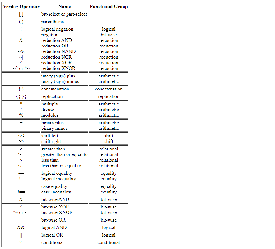
| #bits | Dec Range | Hex Range |
|---|---|---|
| 1 | 0-1 | 0h-1h |
| 2 | 0-3 | 0h-3h |
| 3 | 0-7 | 0h-7h |
| 4 | 0-15 | 0h-fh |
| 5 | 0-31 | 0h-1fh |
| 6 | 0-63 | 0h-3fh |
| 7 | 0-127 | 0h-7fh |
| 8 | 0-255 | 0h-ffh |
| 9 | 0-511 | 0h-1ffh |
| 10 | 0-1,023 | 0h-3ffh |
| 11 | 0-2,047 | 0h-7ffh |
| 12 | 0-4,095 | 0h-fffh |
| 13 | 0-8,191 | 0h-1fffh |
| 14 | 0-16,383 | 0h-3fffh |
| 15 | 0-32,767 | 0h-7fffh |
| 16 | 0-64,535 | 0h-f_ffffh |
| 17 | 0-131,071 | 0h-1_ffffh |
| 18 | 0-262,143 | 0h-3_ffffh |
| 19 | 0-524,287 | 0h-7_ffffh |
| 20 | 0-1,048,575 | 0h-f_ffffh |
| 21 | 0-2,097,151 | 0h-1f_ffffh |
| 22 | 0-4,194,303 | 0h-3f_ffffh |
| 23 | 0-8,388,607 | 0h-7f_ffffh |
| 24 | 0-16,777,215 | 0h-ff_ffffh |
| 25 | 0-33,554,431 | 0h-1ff_ffffh |
| 26 | 0-67,108,863 | 0h-3ff_ffffh |
| 27 | 0-134,217,727 | 0h-7ff_ffffh |
| 28 | 0-268,435,455 | 0h-fff_ffffh |
| 29 | 0-536,870,911 | 0h-1fff_ffffh |
| 30 | 0-1,073,741,823 | 0h-3fff_ffffh |
| 31 | 0-2,147,483,647 | 0h-7fff_ffffh |
| 32 | 0-4,294,967,295 | 0h-ffff_ffffh |
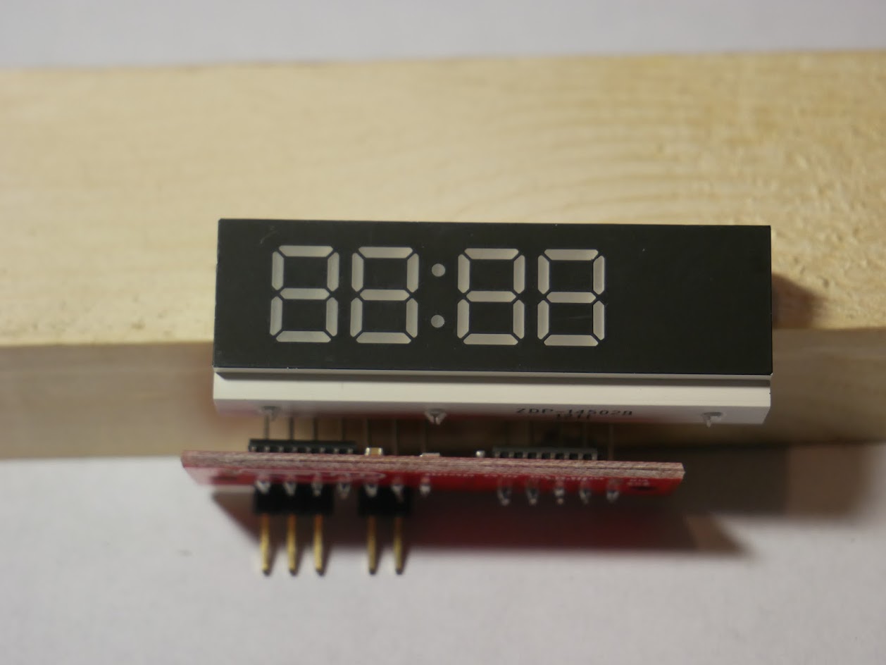
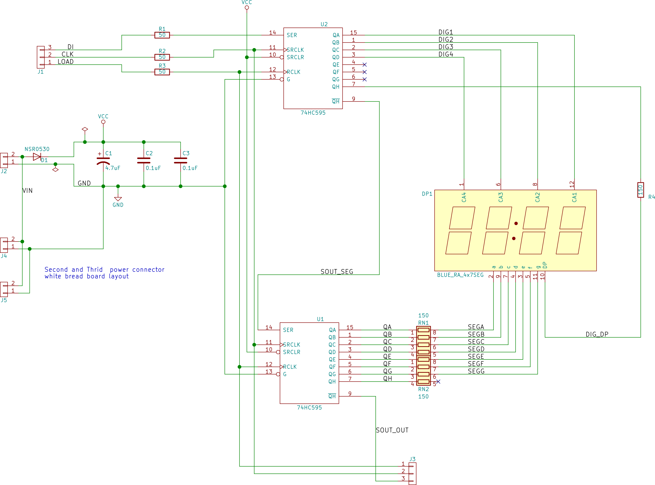
 ## F.2 Blue 4 digit Seven Segment Display (sku CAS-2111)